Semiconductor manufacturing is a complex, precise process creating essential components for modern electronics․ It involves advanced technologies, from crystal growth to thin-film deposition, ensuring high-performance devices․
1․1 Definition and Importance of Semiconductors
Semiconductors are materials with conductivity between conductors and insulators, enabling precise control of electrical current․ Their ability to switch between conducting and non-conducting states makes them indispensable in electronic circuits․ Silicon is the most widely used semiconductor material due to its abundance and versatility․ Semiconductors are integral to modern electronics, including processors, memory chips, and solar panels․ Their development has revolutionized industries, driving advancements in computing, communication, and energy solutions, and underpinning technological progress globally․
1;2 Overview of the Semiconductor Manufacturing Process
The semiconductor manufacturing process is a sophisticated sequence of steps transforming raw materials into functional chips․ It begins with wafer fabrication, involving crystal growth, thin-film deposition, and lithography, followed by precise etching and doping․ Advanced tools and cleanroom environments ensure high purity and accuracy․ The process integrates multiple disciplines, from material science to nanotechnology, to create intricate circuits․ Each step is tightly controlled to meet stringent quality standards, ultimately producing reliable components for diverse electronic applications, from consumer devices to industrial systems․
1․3 Key Steps in Semiconductor Manufacturing
The semiconductor manufacturing process involves several critical steps, starting with crystal growth to produce high-purity silicon ingots, which are then sliced into wafers․ Photolithography transfers circuit patterns onto the wafer using light and photoresist materials․ Etching and doping modify the wafer’s surface to create the necessary electrical properties․ Metallization adds interconnects for circuit completion․ Finally, packaging and testing ensure the chips are functional and ready for integration into electronic devices, adhering to precise quality and performance standards throughout the process․

Wafer Fabrication Process
Wafer fabrication involves creating semiconductor wafers through crystal growth, layer deposition, and precise material processing to form the foundation for integrated circuits․
2․1 Crystal Growth and Wafer Preparation
Crystal growth is the initial stage of wafer preparation, where high-purity silicon ingots are formed through the Czochralski process․ These ingots are then sliced into thin wafers using diamond saws․ The wafers undergo rigorous cleaning and polishing to achieve a mirror-like surface finish, ensuring minimal defects for subsequent semiconductor manufacturing steps․ This process is critical for producing uniform and defect-free starting material for fabricating integrated circuits․
2․2 Epitaxial Growth and Well Formation
Epitaxial growth involves depositing a crystalline layer on a wafer, matching its crystal structure, to create regions with specific electrical properties․ This process, often performed using chemical vapor deposition (CVD), allows precise control over layer thickness and doping․ Well formation follows, where regions are doped to create n-wells or p-wells, defining areas for transistor fabrication․ These steps are critical for achieving the desired electrical performance in semiconductor devices, enabling the creation of complex integrated circuits․
2․3 Active Area Definition and Field Isolation
Active area definition involves creating regions on the wafer where transistors and circuits will be formed․ This is achieved through photolithography, where a pattern is transferred onto the wafer using a photoresist layer․ The exposed areas are then etched to define the active regions․ Field isolation, such as shallow trench isolation (STI), is used to separate these active areas, preventing electrical interference between devices․ These steps ensure precise control over the wafer’s electrical properties, enabling high-density and high-performance semiconductor devices․
CMOS Process Flow
The CMOS process flow is a high-precision method for creating semiconductor devices․ It involves photolithography, etching, and ion implantation to form structures, followed by metallization for interconnects, enabling high-performance devices․
3․1 Photolithography and Pattern Transfer
Photolithography is a critical step in CMOS fabrication, using light to transfer circuit patterns onto silicon wafers․ A photosensitive material, or photoresist, is applied and exposed through a mask․ The exposed areas are then developed, creating a pattern that guides subsequent processes like etching or doping․ This technique ensures precise alignment and miniaturization of semiconductor structures․ Advances in photolithography, such as EUV (extreme ultraviolet) lithography, enable the creation of smaller, more complex transistors, driving advancements in semiconductor technology․ It is essential for achieving high performance and scaling in modern devices․
3․2 Etching and Ion Implantation
Etching removes unwanted material from the wafer, creating precise patterns defined by photolithography․ Techniques like dry or wet etching ensure accurate structure formation․ Ion implantation introduces dopants into the silicon, altering its electrical properties․ This step creates regions with varying conductivity, enabling transistor functionality․ Both processes are critical in CMOS fabrication, ensuring proper device operation․ Advances in these techniques are essential for achieving smaller, faster, and more reliable semiconductor devices, driving technological progress in the industry․
3․3 Metallization and Interconnects
Metal interconnects are deposited to connect semiconductor devices, enabling electrical communication․ Techniques like chemical vapor deposition (CVD) and physical vapor deposition (PVD) are used for metal layer formation․ Interconnects are patterned using photolithography and etching, ensuring precise connections; As transistors shrink, interconnect complexity rises, requiring advanced materials to reduce resistance․ This step is crucial for integrating components and achieving high-performance, reliable circuits in modern CMOS technology․

Thin-Film Deposition and Oxidation
Thin-film deposition involves layering materials like metals and dielectrics on wafers using CVD or PVD․ Oxidation creates insulating layers, crucial for transistor performance and reliability․
4․1 Chemical Vapor Deposition (CVD)
Chemical Vapor Deposition (CVD) is a widely used technique in semiconductor manufacturing for depositing thin films on wafers․ It involves the reaction of precursor gases on a heated substrate, forming high-quality layers such as silicon dioxide or nitride․ CVD offers excellent uniformity and scalability, making it essential for creating insulating and conductive films․ Advanced variations like Low-Pressure CVD (LPCVD) and Plasma-Enhanced CVD (PECVD) further enhance film properties, ensuring precise control over thickness and composition for modern semiconductor applications․
4․2 Physical Vapor Deposition (PVD)
Physical Vapor Deposition (PVD) is a thin-film deposition method in semiconductor manufacturing that involves the transfer of material from a source to a substrate through a vacuum environment․ Techniques like sputtering and evaporation are commonly used․ PVD is ideal for depositing metals and dielectrics, offering high purity and uniformity․ It is widely used for interconnects and barrier layers, ensuring reliable electrical performance․ However, PVD can face challenges in achieving conformal coverage on complex geometries compared to CVD methods․
4․3 Thermal Oxidation and Nitridation
Thermal oxidation and nitridation are critical processes in semiconductor manufacturing for creating high-quality dielectric layers․ Thermal oxidation forms silicon dioxide (SiO₂) on silicon wafers, essential for gate dielectrics and isolation․ Nitridation produces silicon nitride (Si₃N₄) or oxynitride films, offering superior electrical properties․ These processes are performed at high temperatures in controlled atmospheres․ They ensure film uniformity, thickness, and reliability․ However, precise control of temperature and ambient gases is necessary to prevent defects and maintain performance․ These layers are vital for transistor functionality and overall chip reliability․

Process Control and Metrology
Process control and metrology ensure high-quality semiconductor manufacturing by monitoring defects, parametric testing, and advanced metrology tools, crucial for maintaining precision and reliability in chip production․
5․1 Defect Inspection and Yield Enhancement
Defect inspection is a critical step in semiconductor manufacturing, ensuring high-quality products by identifying and classifying defects․ Advanced metrology tools and automated systems monitor wafers, detecting anomalies that could affect performance․ Yield enhancement strategies focus on analyzing defect root causes, optimizing process conditions, and improving equipment performance․ This systematic approach minimizes defects, boosts production efficiency, and ensures consistent, reliable chip output, ultimately driving manufacturing excellence and customer satisfaction in the semiconductor industry․
5․2 Parametric Testing and Process Monitoring
Parametric testing and process monitoring ensure semiconductor manufacturing processes operate within precise specifications․ These steps measure key parameters like thickness, resistance, and doping levels, using advanced metrology tools․ Real-time data from sensors and equipment is analyzed to detect deviations, enabling prompt corrections․ This continuous oversight maintains process stability, optimizes yield, and ensures compliance with quality standards․ By integrating automated systems, manufacturers achieve higher efficiency and consistency, crucial for producing reliable, high-performance semiconductor devices in today’s competitive market․
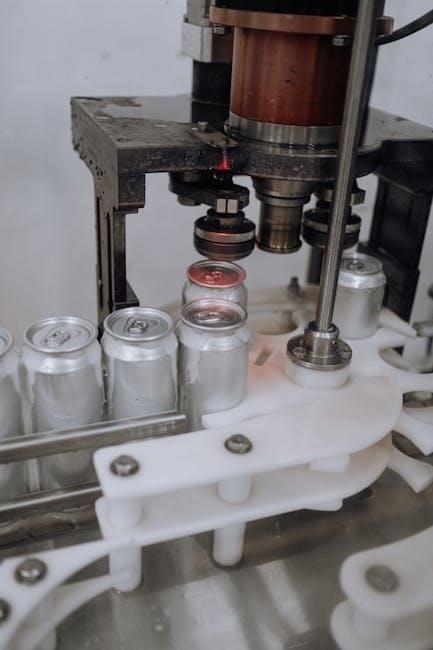
Packaging and Assembly
Packaging and assembly involve wafer dicing, die preparation, and package assembly․ Techniques like wire bonding and encapsulation protect the die, ensuring reliable connections and durability in devices․
6․1 Wafer Dicing and Die Preparation
Wafer dicing is the process of separating individual semiconductor dies from a wafer․ It involves scribing or laser cutting along predefined lines․ After dicing, dies are cleaned and inspected for defects․ Die preparation includes backside grinding to thin the substrate, ensuring proper adhesion during packaging․ This step is critical for producing functional semiconductor devices, ready for assembly into packages․ Precision and care are essential to maintain die integrity and performance․
6․2 Package Assembly and Wire Bonding
Package assembly involves encapsulating the semiconductor die in a protective material, ensuring durability and reliability․ Wire bonding connects the die to the package leads using thin metal wires․ The process includes attaching the die to a lead frame or substrate, applying an encapsulant for protection, and sealing the package․ Advanced packaging techniques, such as flip-chip and 3D stacking, enhance performance․ Wire bonding is critical for establishing electrical connections, while underfill materials reduce stress during temperature changes․ This step prepares the semiconductor for final testing and deployment in electronic devices․
6․3 Final Testing and Quality Assurance
Final testing ensures semiconductor devices meet performance and reliability standards․ This includes probe testing, parametric testing, and functional testing to verify electrical specifications․ Quality assurance involves rigorous inspections and certifications to ensure compliance with industry standards․ Environmental stress testing, such as temperature and humidity tests, evaluates long-term durability․ Automated systems and advanced metrology tools are used to detect defects and ensure consistency․ This critical step guarantees that only high-quality semiconductors are delivered for use in electronic devices, maintaining customer trust and product reliability․
The semiconductor industry continues to evolve, driven by advancements in AI, machine learning, and new materials like SiC and GaN․ Future trends include enhanced process optimization, sustainable manufacturing, and the adoption of 3D chip stacking․ Investments in cutting-edge technologies and global collaborations will shape the next generation of semiconductor production, ensuring smaller, faster, and more efficient devices for emerging applications․
7․1 Advances in Semiconductor Manufacturing Technology
Recent advancements in semiconductor manufacturing focus on improving chip performance and reducing size․ EUV lithography enables precise patterning for 5G and AI chips․ 3D chip stacking enhances integration, while new materials like SiC and GaN boost power efficiency․ AI-driven optimization streamlines processes, reducing defects and costs․ These innovations address global demand for faster, smaller, and more efficient devices, driving the industry toward sustainable and scalable solutions․
7․2 Role of AI and Machine Learning in Process Optimization
AI and machine learning are revolutionizing semiconductor manufacturing by optimizing complex processes․ Predictive analytics and real-time monitoring enable defect detection and yield enhancement․ ML algorithms analyze sensor data to predict process deviations, allowing proactive adjustments; AI-driven tools also optimize material usage and equipment performance, reducing costs․ By bridging design and manufacturing, these technologies accelerate innovation and improve scalability, ensuring high-quality chip production in a rapidly evolving industry․